
Abstract
TiN thin film electrodes for supercapacitors were deposited successfully on textured silicon substrates by reactive magnetron sputtering and silicon surface texturization. The areal specific capacitance of the rough TiN electrodes was nearly two-fold higher than that of the smooth electrodes. Meanwhile, the textured TiN electrodes exhibit rough surfaces comprising a large number of random pyramids and good cycling stability with about 28% decay in capacitance value after 3500 cycles. In addition, the rough electrodes also exhibit relatively favorable charge transfer and ion diffusion due to their higher effective surface area. These results demonstrate that TiN electrodes on textured silicon substrates will have promising prospects for high-performance supercapacitors.
Export citation and abstract BibTeX RIS
The increasing demands for integrated and miniaturized multifunctional electronic devices stimulate the sustainable development of a variety of micro-size power sources and relevant technologies.1,2 Among energy storage systems, supercapacitors, also called electrochemical capacitors, have attracted great attention owing to their high-power density, long-term cycle stability, and fast charge/discharge rate.3,4 An advanced electrode material becomes a key factor for developing high-performance supercapacitors. Currently, interesting electrode materials used for supercapacitors are mainly carbon materials and transition metal oxides.5 Carbon materials have become one of the most widely studied and most promising electrodes in electrical double-layer capacitors (EDLCs) due to their low cost, high conductivity, and excellent cycling stability, however, their specific capacitance and energy densities are generally low.6,7 Pseudocapacitors using transition metal oxides can achieve higher energy density than that of EDLCs, whereas transition metal oxides suffer from low power density and poor cycling stability.8 The most representative transition metal oxides such as RuO2 and IrO2 are relatively rare and expensive, which limit their large-scale use.9
Recently, transition metal nitrides, such as TiN, VN, or MoNx, have emerged as potential candidates for supercapacitors because of their low cost, high electronic conductivity, and superior chemical resistance.10 Among the various nitrides, TiN, with superior electrical conductivity, high corrosion resistance, and good electrochemical performance, has been found to be suitable for electrodes for microelectronic devices11 and electrochemical capacitors.12 For the preparation process, note that TiN electrodes fabricated with powders usually have some drawbacks such as bad adhesion to the current collector, additional external resistance, and incompatibility with standard micro-fabrication processes.13 Nanostructured TiN films using physical vapor deposition (PVD), widely used in the field of semiconductor technology, can serve as alternative electrodes to overcome the above mentioned drawbacks.
In PVD technology, reactive DC magnetron sputtering can produce films with porous nanostructures, high purity, good adhesion, and controlled thickness.14 For example, porous VN films are deposited on smooth silicon substrates by reactive DC magnetron sputtering.15 The areal capacitance values increase with increasing film intracolumnar and intercolumnar porosity. Such an increase in capacitance is due to their high effective specific areas which can react with the electrolytes. The highest energy and power densities obtained for VN interdigitated planar micro-supercapacitors are 2 μWh cm−2 and 10 mW cm−2, respectively, and the electrodes exhibit good capacitance retention (10000 cycles). Achour et al. investigated the effect of parameters on the capacitance behavior of TiN films.13 It is found that the specific areal capacitances enhance from 0.28 up to 8.8 mF/cm2, when the film thickness increases from 180 to 2240 nm. The increasing areal capacitance should be attributed to the enhanced mass loading. The introduction of high mass loading of film electrodes require the film to be deposited for a long time leading to a quick consumption of target. Therefore, it is more preferable to enhance the specific areal capacitance by increasing the effective specific area with limited thickness.
For solar cells, texturing techniques of silicon substrate have been generally utilized to increase surface area, whereby light trapping can be enhanced significantly.16 We believe that if the TiN film is deposited on textured Si silicon, the effective surface area can be significantly increased. This can provide more active adsorption sites and promote the electrolyte diffusion resulting in an increasing specific capacitance.
Experimental
Surface treatment of monocrystalline silicon
The p-type Si(100) wafers (100 mm diameter, 500 μm thickness) were cut into 20 × 20 mm square pieces for future investigation. The silicon substrates were first subjected to a standard RCA cleaning process to eliminate any impurities, including particles, organic, metal, etc. Then the ultra-clean substrates were saw-damage etched with 20 wt% NaOH solution at 80°C for 2 min to remove surface defects and damage. The surface texturization of monocrystalline silicon was accomplished using mixed aqueous solutions including 1.5 wt% NaOH, 4 wt% NaSiO3 and 6 vol% ethanol at 85°C for 20–40 min. For comparison, the smooth silicon substrates after RCA cleaning were also employed in this work.
Thin film deposition
TiN thin films were deposited on the smooth or texturized silicon substrates by DC reactive magnetron sputtering of Ti metal target (purity of 99.999%). The distance between target and substrate was kept constant at 60 mm. The sputtering chamber was initially pumped down to a base pressure of 3 × 10⁻⁴ Pa. Under working conditions, the gas pressure rose to 0.5 Pa at a gas flow of 2.5 sccm N2 and 30 sccm Ar controlled by a gas flow controller and throttle valve. The target was pre-sputtered for 10 min to remove surface contamination and then sputtered on silicon substrates for 20 and 30 min. The deposition was performed at the sputtering power of 113 W and substrate temperature of 350°C for all the experiments. The synthetic procedure of TiN thin films was shown in Fig. 1.
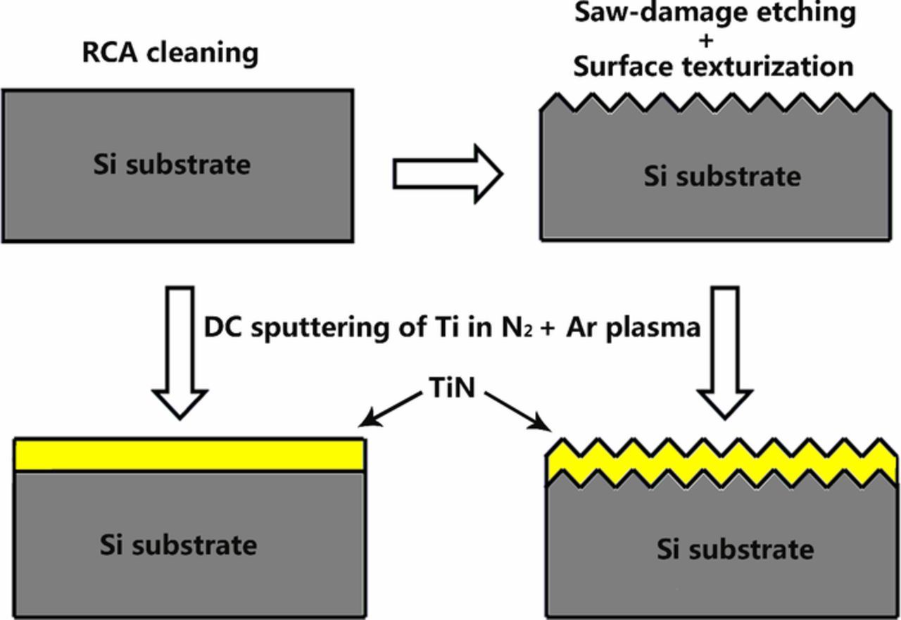
Figure 1. Schematic illustration of the fabrication process for TiN thin films.
Characterizations
Phase structure analysis of TiNx thin films was carried out with grazing incidence X-ray diffraction (GIXRD, Empyrean, PANalytical) using Cu Kα radiation (λ = 1.54 Å) operated at 40 kV and 40 mA. The film thickness was measured by a step profiler. The surface appearance of films on substrates was observed using a confocal laser scanning microscope (CLSM, LEXT OLS4000, OLYMPUS). The surface micro-topography of TiN thin films was revealed using focused ion beam-scanning electron microscopy dual beam system (FIB-SEM, Helios G4 UX, Thermo). The chemical bonding states of TiN thin films are examined by X-ray photoelectron spectroscopy (XPS, ESCALAB 250Xi, ThermoFisher). The electrochemical measurements were carried out on a CHI 760E electrochemical workstation using a conventional three-electrode set-up in 1 M KCl aqueous electrolyte solution. The three-electrode system consists of the thin film working electrode (effective area 2 × 1 cm2), Pt counter electrode and saturated calomel reference electrode (in saturated KCl), respectively. Cyclic voltammogram (CV) and galvanostatic charge-discharge were conducted in 1 M KCl electrolyte at room temperature. Electrochemical impedance spectra (EIS) were measured from 100 kHz to 0.01 Hz with an AC voltage amplitude of 5 mV at the open circuit potential. Prior to each test, potential-time was carried out for 30 min under open circuit. If the potential fluctuation was in the range of ±3 mV, the test system was in a steady-state, and the electrochemical measurement was continued.
Results and Discussion
Figure 2 depicts the surface appearance of TiN films on silicon substrates textured for 0, 20, and 40 min, respectively. The TiN films on substrates after only RCA cleaning were quite smooth and featureless while the films on textured substrates show a large number of random pyramids. These pyramids are produced by anisotropic etching of silicon, which is caused by the difference of the etch rates in the (100) and (111) directions. In alkaline solutions, the etch rate in the (111) direction is much lower than that in the (100) direction due to the larger density of the plane in the (111) direction.17 The effective specific surface area of the substrate is estimated by a sum of the side area of pyramid-like grains from the morphology of surface area as seen in Fig. 2. Compared with smooth silicon, the effective surface area of the substrate increases by a factor of two when the silicon substrate is textured for 20 min. As the texturing time prolongs, the size of the pyramids and etching depth of the substrates are improved, leading to larger specific surface area of TiN films. However, the uniformity and coverage rate of pyramids decrease with increasing texturing time. This results in a reduction of effective surface area (from 2 to 1.35 fold).
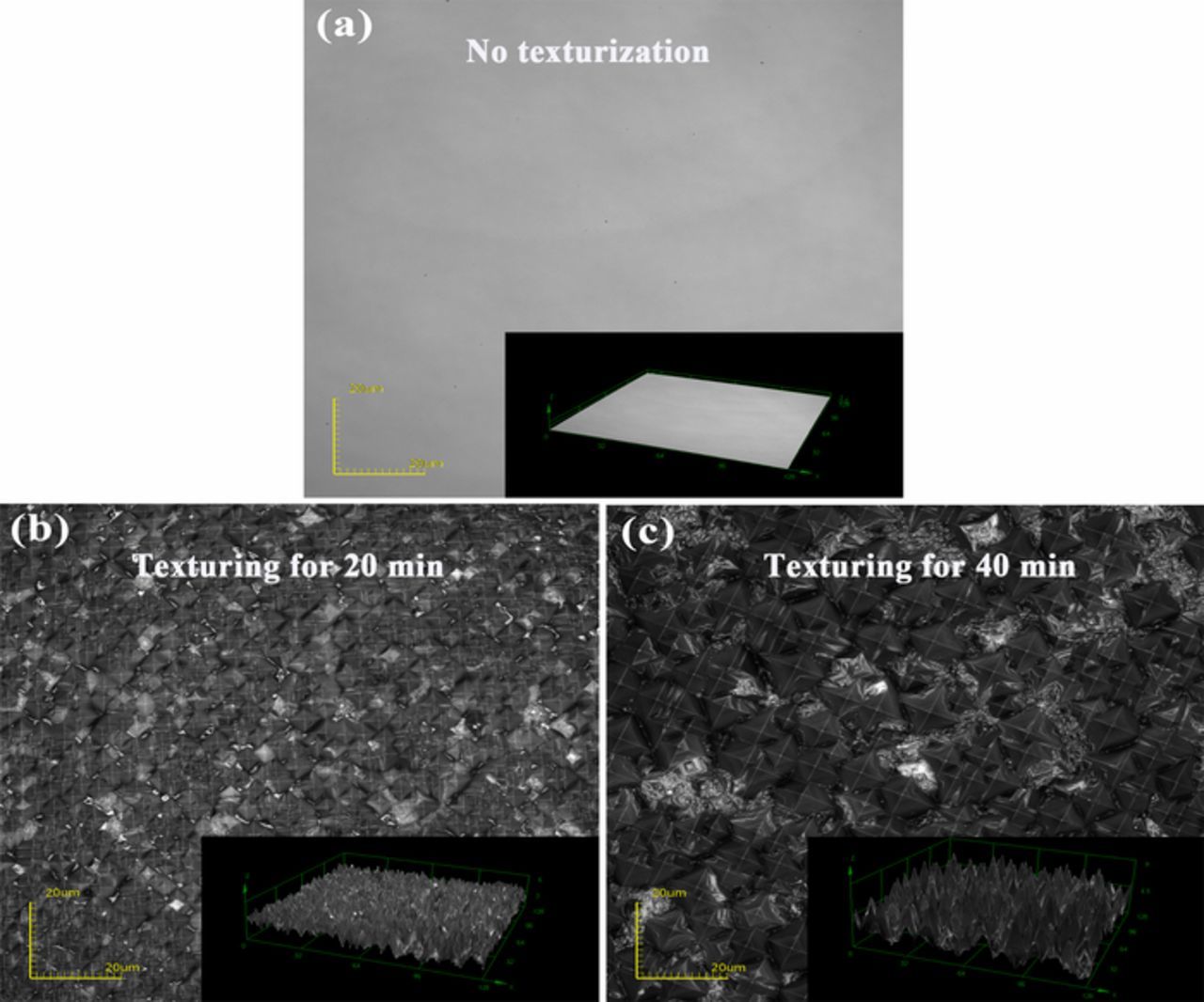
Figure 2. Surface appearance of TiN films on silicon substrates textured for (a) 0 min, (b) 20min and (c) 40 min.
The XRD pattern of DC reactive sputtered TiN thin films in Fig. 3a exhibits an (111)-preferred orientation and good degree of crystallization. The (111) plan is known to exhibit the lowest strain energy. Three characteristic peaks at 2θ = 36.98°, 42.90°, and 62.54° correspond to the (111), (200), and (220) planes of the fcc TiN, respectively. Surface micro-structures of TiN thin films are displayed in FIB-SEM images, as shown in Fig. 3b. It can be obviously observed that the thin films possess the even pyramidal shaped grains and relatively loose structure. The mean grain size is approximately 25 nm. The XPS spectra of the films are shown in Figs. 3c and 3d. The peak deconvolutions exhibit major components mixture of TiN, TiO2, and titanium oxynitride impurities. The XPS spectra of Ti 2p can be mainly deconvoluted into four peaks. The intense peaks located at about 454.1, 455.0, 457.0, and 462.6 eV are related to Ti 2p3/2, while the peak at lower binding energies of 460.2 eV is assigned to Ti 2p1/2. The components at binding energy values of 455.0 and 460.2 eV are very close to those reported for stoichiometric TiN, whereas the binding energy value of 457.0 eV is identical to Ti 2p3/2 of TiOxNy.13 The peak at higher energy can be assigned to TiO2.18 The component at binding energy value of 454.1 eV is assigned to TiNx (x < 1) based on that for a TiNx (x = 0.81 or 0.92) standard sample. From the XPS spectra of N 1s, it can be noted that the peaks at around 396.3 and 399.0 eV correspond to TiN and TiOxNy, respectively. This result is similar to that we reported recently.18 It is reported that TiOxNy would have an important role in the capacitance of our films which will be described subsequently.
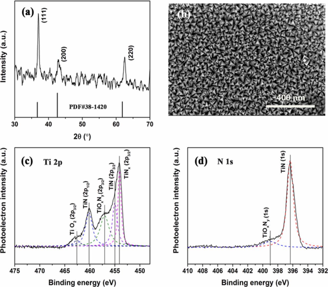
Figure 3. (a) XRD pattern of TiN thin films, (b) FIB images of TiN films, (c) Ti 2p XPS spectra and (d) N 1s XPS spectra.
Figure 4 is the cyclic voltammetry (CV) curves of TiN thin film electrodes tested in 1.0 M KCl aqueous solution at a scan rate of 0.005–0.2 V·s−1 and potential window of -0.4–0.4 V versus a saturated calomel electrode (SCE). In addition, the thicknesses of TiN thin films sputtered for 20 and 30 min are estimated to be ∼208 nm and ∼296 nm with a step profiler. It can be seen that all of the CV curves of TiN electrodes exhibit a nearly symmetrical rectangular shape, indicating a quasi-ideal capacitive behavior. Obviously, in comparison to the smooth TiN electrodes, the textured electrodes have much higher current density. It has been demonstrated that the capacitance of TiN electrode arises from both electric double layer (EDL) capacitance and pseudocapacitance. The latter is due to a faradaic reaction.19 The faradaic interfacial reaction on oxidized TiOxNy can be expressed as
![Equation ([1])](https://content.cld.iop.org/journals/1945-7111/166/15/H802/revision1/d0001.gif)
The intercalation and deintercalation of cations may take place as well, which have been proposed as a charge storage mechanism of MnO2 pseudocapacitance.20 Based on these CV curves, the areal specific capacitance of TiN electrodes can be calculated as21
![Equation ([2])](https://content.cld.iop.org/journals/1945-7111/166/15/H802/revision1/d0002.gif)
where Cs, s, v, and △V denote areal specific capacitance (F·cm−2), the effective area of electrode material (cm2), the potential scan rate (V·s−1) and the potential window (V), respectively. ∮idV is the voltammetric charge, that is, integral area of current-voltage (CV) curves. The areal specific capacitances of these electrodes are plotted as a function of scan rate in Fig. 5. The areal specific capacitance decreases gradually and tends to be stable for all electrodes when scan rates increase from 0.005 V·s−1 to 0.2 V·s−1. As is shown in Fig. 5a, rough film electrodes on textured silicon substrates exhibit the increased areal capacitance than smooth electrodes mainly due to their larger specific surface area which provides more active adsorption sites. However, the electrodes on substrates textured for 40 min have lower capacitance than those on substrates textured for 20 min resulting from their lower uniformity and coverage rate of pyramids. In Fig. 5b, the similar variation of specific capacitance with the texturing time is found for 296 nm thick TiN electrodes. Furthermore, the enhanced thickness of TiN films results in an increase of the areal specific capacitance. Commonly, the capacitance of the electrodes on silicon substrates textured for 20 min is near two-fold higher than that of the smooth electrodes. Eventually, the area specific capacitance of 296 nm thick electrodes on substrates textured for 20 min achieves a maximum value of 10.1 mF·cm−2, corresponding to the scan rate of 0.005 V·s−1.
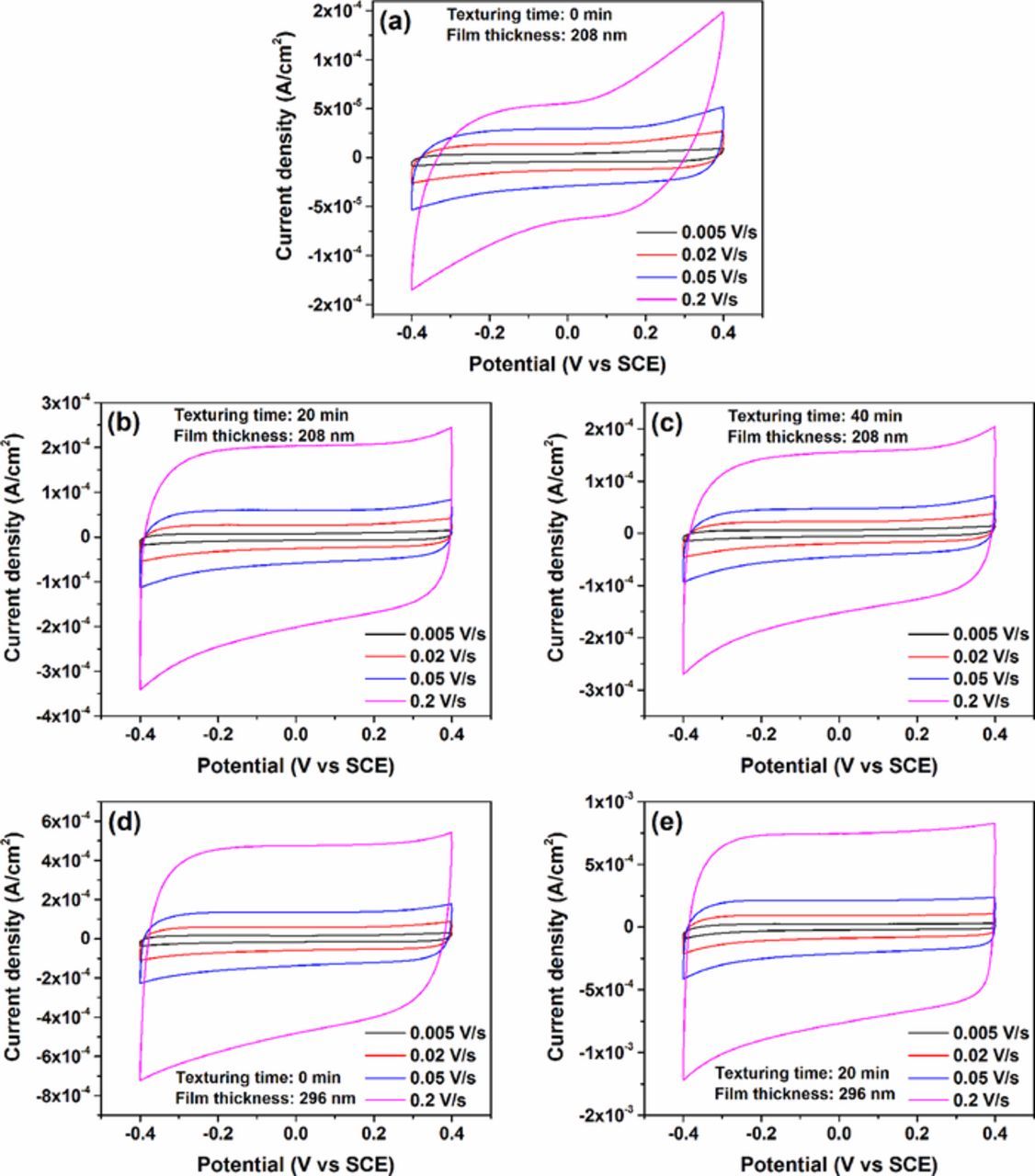
Figure 4. Cyclic voltammetry curves of 208 nm thick TiN electrodes on silicon substrates textured for (a) 0 min, (b) 20min and (c) 40 min, and 296 nm thick TiN electrodes on silicon substrates textured for (d) 0 min and (e) 20min.
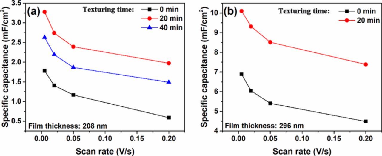
Figure 5. Comparison of areal capacitance of (a) 208 nm thick TiN electrodes deposited on silicon substrates textured for 0 min, 20min and 40 min and (b) 296 nm thick TiN electrodes grown on silicon substrates textured for 0 min and 20 min.
As mentioned above, the CV characterization gives an unlinear relation between the current and scan rate. This might be attributed to the contribution of diffusion controlled redox reactions.20 The total capacitance can be deconvoluted into a surface-dominant process corresponding to the case i(v)∝v, encompassing double-layer charging and the pseudocapacitive charge transfer at Ti3+/4+ centers, and a diffusion-controlled process corresponding to the case i(v)∝v1/2.20 The total current tested at a constant scan rate, i(v), can be given by
![Equation ([3])](https://content.cld.iop.org/journals/1945-7111/166/15/H802/revision1/d0003.gif)
where both k1 and k2 are sweep rate independent constants. These values can be obtained from fitting the  and v1/2 using
![Equation ([4])](https://content.cld.iop.org/journals/1945-7111/166/15/H802/revision1/d0004.gif)
Thereafter, the capacitive effect and diffusion-controlled intercalation processes can be distinguished quantitatively as shown in Fig. 6. Note that the surface-dominant capacitance is calculated as 4.6 mF·cm−2 for 296 nm-thick TiN electrodes grown on substrates textured for 20 min at 200 mV/s, and this value is nearly constant when the scan rate decreases to 5 mV/s. However, the diffusion-controlled capacitance is scan rate dependent, increasing with decreasing the scan rate.
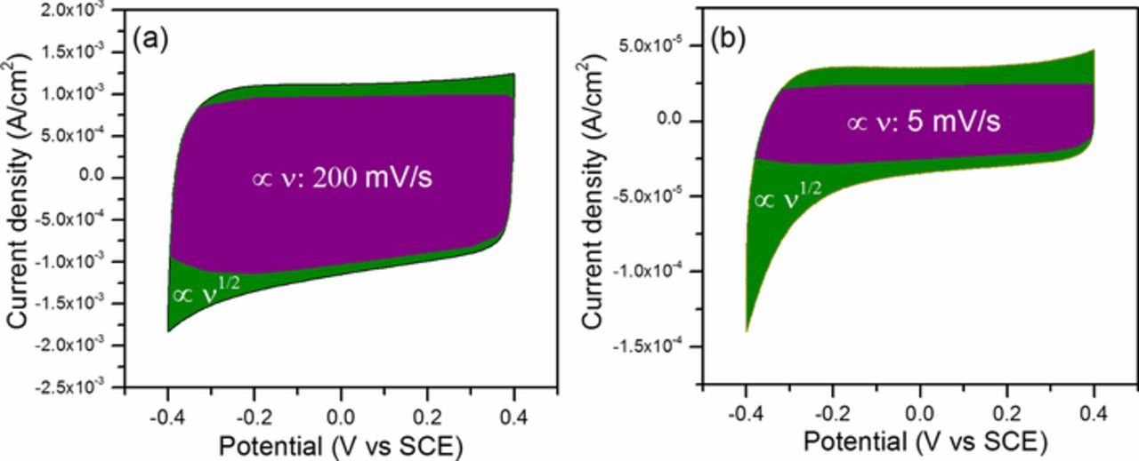
Figure 6. Deconvolution of two capacity components: surface-dominant capacity (∝v, purple) and diffusion-controlled intercalation capacity (∝v1/2, olive). CVs at 200 mV/s (a) and 5 mV/s (b) for 296 nm-thick TiN films grown on silicon substrates textured for 20 min.
The electrochemical capacitance properties of TiN electrodes are also evaluated via galvanostatic charge-discharge measurements. Figure 7 shows the charge-discharge curves of TiN films tested at different current densities. It can be seen that the charge-discharge curves exhibit a nearly isosceles triangle shape and are gradually prolonged with decreasing current density, revealing a good capacitive behavior. The areal specific capacitance of TiN electrodes can be calculated using
![Equation ([5])](https://content.cld.iop.org/journals/1945-7111/166/15/H802/revision1/d0005.gif)
where Cs, I, td, and ΔV denote the areal specific capacitance (F·cm−2), the current density (mA·cm−2), discharge time (s) and charge-discharge voltage (V). Figure 7f presents the specific capacitances of TiN films plotted as a function of the current density. Note that the specific capacitances decrease gradually and then reach a stable level with increasing the current density. Comparatively, the specific capacitances of 208 nm thick films grown on 20 min textured silicon substrates are much higher than that of 208 nm thick films grown on smooth silicon substrates. As the texturing time increases to 40 min, however, the specific capacitance decreases, which is ascribed to the lower uniformity and coverage rate of pyramid-like TiN grains. A similar trend of change in specific capacitances is also observed when the film thickness increases to 296 nm. These results are in good agreement with the aforementioned CV measurements. For a 296 nm electrode deposited on 20 min textured substrate, the highest areal capacitance of 10 mF/cm2 is achieved. This value is higher than that of 980 nm thick TiN electrode in 0.5 M K2SO4 electrolyte (9.2 mF/cm2 at 2 mV/s).13
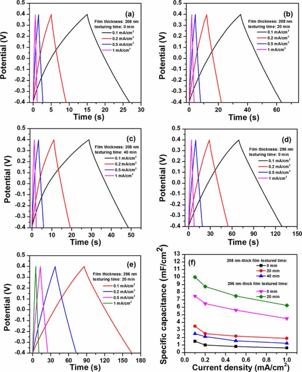
Figure 7. Galvanostatic charge-discharge curves of 208 nm thick TiN electrodes deposited on silicon substrates textured for (a) 0 min, (b) 20 min and (c) 40 min, and 296 nm thick TiN electrodes grown on silicon substrates textured for (d) 0 min and (e) 20min; (f) corresponding areal capacitance with respective to current density.
Figure 8 displays the Ragone plot of the areal energy and power densities for the 296 nm thick TiN electrodes deposited on textured substrates, where the results of transition metal nitrides electrodes with similar thicknesses tested in aqueous electrolyte are also given for comparison. This performance of our electrode is evaluated using single electrode capacitance obtained from charge-discharge measurements. The areal capacitance (Cdevice) of the full device is calculated using
![Equation ([6])](https://content.cld.iop.org/journals/1945-7111/166/15/H802/revision1/d0006.gif)
where CS is the areal capacitance of single electrode obtained from Eq. 5. The areal energy density (EA, Wh cm−2) and power density (PA, W cm−2) are calculated by
![Equation ([7])](https://content.cld.iop.org/journals/1945-7111/166/15/H802/revision1/d0007.gif)
![Equation ([8])](https://content.cld.iop.org/journals/1945-7111/166/15/H802/revision1/d0008.gif)
where ΔV and Δt denote the charge-discharge voltage (V) and discharge time (s), respectively. The obtained energy density of 0.22 μWh cm−2 and power density of 100 μW cm−2 are at least ten orders of magnitude larger than the values for 180 nm-thick TiN films in H2SO4.13 The maximum energy density is about two orders of magnitude larger than that of 500 nm-thick TiN/CNTs in H2SO4.22 The performance of our TiN electrodes on textured substrates is also comparable to those of interdigitated VN electrodes.15
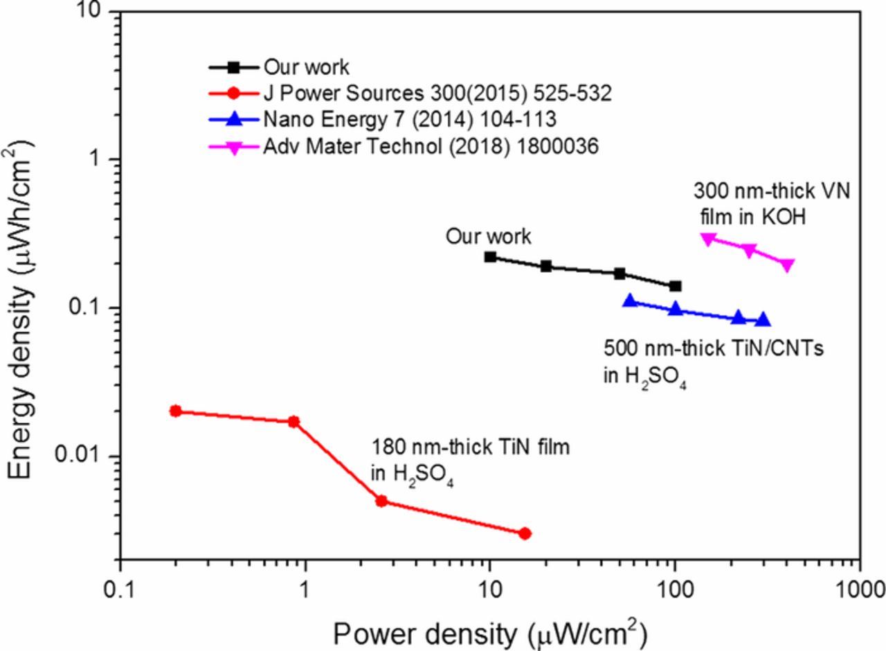
Figure 8. Ragone plots of the 296 nm thick TiN electrodes with energy and power performance. These performances are calculated from the areal capacitance of single electrode of 296 nm-thick TiN films. Reported values for other transition metal nitrides electrodes with similar thicknesses are also added for comparison. The performances of 180 nm-thick TiN films and the 500 nm-thick TiN/CNTs are calculated from the areal capacitance of single electrode. The performance of 300 nm-thick VN refers to interdigitated microdevice.
Cycling stability is one of the most critical requirement for supercapacitor applications.23 Figure 9 shows the cycling performance of our TiN electrodes by CV test at a scan rate of 0.2 V·s−1. The specific capacitance of TiN electrodes suffers from a drastic increase within their first 100 cycles and then reduces extremely slowly, ending up with about 28% loss after 3500 cycles.
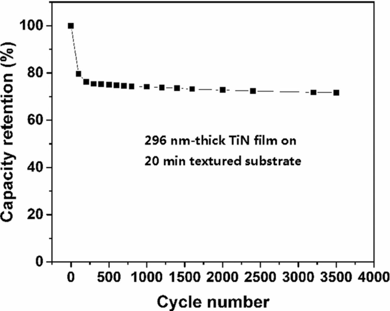
Figure 9. Cycling performance of 296 nm thick TiN electrodes on substrates textured for 20 min at a scan rate of 0.2 V·s−1 for 3500 cycles.
To understand the origin of the capacitance degradation, the changes in chemical states of TiN electrodes before and after the cycling test were examined by XPS analyses. Figure 10 displays the Ti 2p and N 1s XPS spectra of 296 nm thick TiN electrodes on substrates textured for 20 min after 3500 cycles. It can be clearly observed that the peak intensity of TiO2 compound increases after 3500 cycles, while the intensities of nitride component (TiN and TiOxNy) peaks decrease. Likewise, the TiN and TiOxNy in N 1s XPS peaks also decrease after long-time electrochemical treatment. These results indicate that the instability of TiN electrode is attributed to the irreversible electrochemical oxidation reaction in KCl aqueous solution24,25
![Equation ([9])](https://content.cld.iop.org/journals/1945-7111/166/15/H802/revision1/d0009.gif)

The resulting TiO2 layer is much less electrochemically active due to a stable valance state of Ti4+ in a basic solution.24,25 Hence, it causes a capacitance loss for the TiN film electrode.
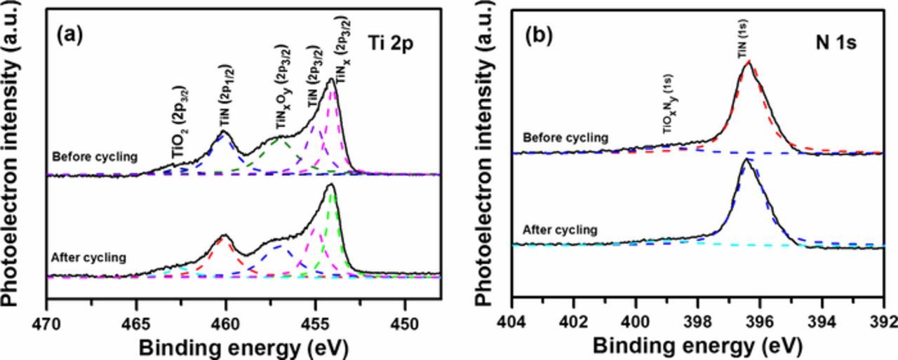
Figure 10. (a) Ti 2p XPS spectra and (b) N 1s XPS spectra of TiN films taken before and after 3500 cycles.
In order to investigate the charge transfer and ion diffusion properties of the TiN thin film electrodes, the electrochemical impedance spectroscopy (EIS) was measured. The Nyquist plots shown in Fig. 11a demonstrate a semicircle at the high frequency and a straight slopping line at low frequency. The smaller radius of the semicircle for the rough film electrodes indicates that the charge-transfer resistance (Rct) of the textured TiN electrode is much less than that of the smooth TiN electrodes.26 Moreover, the charge-transfer resistance (Rct) of 296 nm thick textured TiN electrode is smaller than that of 208 nm thick textured TiN electrode. The straight slopping lines of the smooth and rough electrodes with different thicknesses, present a partial capacitive-type behavior with favorable ionic diffusion. Figure 11b illustrates a comparison of the Bode plots of the smooth and rough electrodes. Two time constants are found approximately from the Bode spectra. The characteristic frequency f at −45° phase angle is 3.56 HZ for 296 nm thick smooth TiN electrodes, which is lower than that of textured TiN electrodes with thickness of 208 nm (5.9 HZ), 296 nm (7.8 HZ). The corresponding time constant (τ) is the minimum time needed to discharge all of energy from the device with an efficiency of greater than 50%.27 It can be calculated by
![Equation ([10])](https://content.cld.iop.org/journals/1945-7111/166/15/H802/revision1/d0011.gif)
where f is the frequency. The τ values of the 296 nm-thick TiN electrodes deposited on smooth and textured silicon substrate are calculated to be 44.7 and 20.4 ms, in comparison with 27 ms for the 208 nm thick TiN electrodes deposited on textured silicon substrate. The TiN electrodes deposited on textured silicon substrates exhibit a lower time constant than TiN film formed over the pristine silicon substrate due to their lower ionic resistance which would be discussed subsequently.28 The EIS spectra are thus fitted by the equivalent circuit in inset of Fig. 11a, where Rs, Rct, CPE1, CPE2, and W represent the total resistance of electrolyte and electrode, the faradaic interfacial charge-transfer resistance, the double layer capacitance, pseudocapacitance, and Warburg impedance, respectively.29 The equivalent circuit elements calculated by fitting the equivalent circuit are summarized in Table I. The equivalent series resistance, Rs, is comparable for all electrodes because of similar electrolyte resistance, contact resistance, and electrode resistance. The Rct of the rough TiN electrodes is several times lower than that of the smooth electrodes, which demonstrates much lower ionic resistance of the textured TiN electrodes. W is the Warburg impedance that can be expressed as W = Y− 10(jw)− 0.5, where Y0 is the Warburg coefficient. It is determined as 0.13 S·s5·cm−2 for no textured electrode, whereas for 208 and 296 nm thick textured TiN electrodes, it is 0.156 and 0.2 S·s5·cm−2, respectively. The CPE is the constant phase element that is defined as follows: ZCPE = Y− 10(jw)− α (0 ⩽ α ⩽ 1), where j and w are the imaginary unit and angular frequency, respectively. Y0 and α are frequency-independent CPE parameters.30 Compared to smooth electrodes, the textured TiN electrodes exhibit a more ideal capacitive behavior with somewhat higher CPE and n, which may be due to their much higher effective surface area.
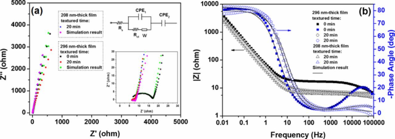
Figure 11. (a) Nyquist and (b) Bode plots of TiN electrodes with different thicknesses on substrates textured for 0 min and 20 min.
Table I. Model fitting parameters of TiN electrodes.
| Element | Smooth TiN | Rough TiN (296 nm) | Rough TiN (208 nm) |
|---|---|---|---|
| Rs (Ω·cm2) | 6.262 | 5.812 | 5.92 |
| CPE1-Yo (S·sn1·cm−2) | 3.6 × 10⁻² | 1.52 × 10⁻³ | 4.4 × 10⁻³ |
| n1 (0<n<1) | 0.6815 | 0.8426 | 0.8 |
| CPE2-Yo (S·sn2·cm−2) | 0.0029 | 0.0002 | 0.0017 |
| n2 (0<n<1) | 0.816 | 0.92 | 0.91 |
| W- Yo (S·s5·cm−2) | 0.13 | 0.2 | 0.156 |
| Rct (Ω·cm2) | 11.26 | 3.24 | 3.728 |
Conclusions
TiN thin film electrodes with different thickness were prepared successfully on the smooth and textured silicon substrates by reactive magnetron sputtering. The areal specific capacitance of the textured TiN electrodes was double that of the smooth electrodes because of their excellent electrical conductivity, rough structure composed of many random pyramids, and higher specific surface area. Moreover, the enhanced thickness of TiN films resulted in an increase of the areal specific capacitance but unaffected the variation trend of specific capacitance with the surface roughness of electrodes. After 3500 cycles, the textured TiN with the highest specific capacitance of 10.1 mF·cm−2 at 0.005 V·s−1 also demonstrated reasonable capacitance retention of 72%. In addition, the textured electrodes were more favorable for charge transfer and ion diffusion due to their higher effective surface area, although they exhibited slightly non-ideal capacitive behavior. These results suggest that TiN electrodes on textured silicon substrates could be used as a promising and innovative electrode material for high-performance supercapacitors.
Acknowledgments
N. S., X. M., and D. Z. were supported by the National Natural Science Foundation of China (grant No. NSFC 51672032 and 51972037), the Fundamental Research Funds for the Central Universities of China (No. DUT17ZD211). Y. S., P. J. and Y. Z. were financially supported by the Science and Technology Major Project of Sichuan Province, China (No. 2018SZDZX0012).
ORCID
Dayu Zhou 0000-0001-5143-9230